
The current sensing card is responsible for measuring the output current from the inverter. Further, it should condition the measured value and prepare it for direct input to an analog to digital converter (ADC) which is located on a dedicated PCB.
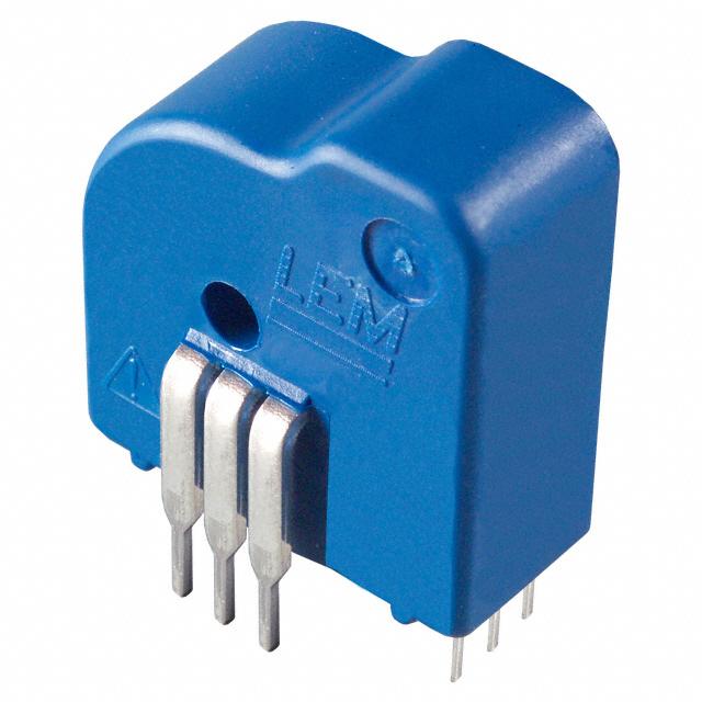
The LEM LTS 25-NP current sensor.
The measured current can either pass in a wire through the center hole, or connect to the main legs via circuit board paths.
To measure the current, special hall effect sensors are employed; LEM LTS 25-NP.
I will not go into details about the hall measurement principle in this post (Eirik has already covered it quite well), but will simply provide a few images and schematics.The sensor can measure nominal current up to 25 A, and peak currents (e.g. during short circuits) up to 80 A.
The dedicated current sensing card features three such sensors along with three auxiliary circuits to condition the signal. Potmeters are employed to fine tune measurements and cancel any offsets.
As the sensors requires 5 V operating voltage and the opamps +-15V, two power supplies are needed from a separate power supply card (I'll make a post of it as soon as the design is ready).
The logic and way-of-thinking is very similar to the one presented in Step-by-step post about the voltage sensing card, so let's jump right to the schematics. Note that output phases are denoted according to European standard: U, V and W for phase 1, 2 and 3 (or a, b, c as some Americans prefer).
The complete schematics for the current sensor card
The perceptive reader might notice the missing resistors in the opamp feedback. This is because it is used as a buffer, i.e. used to duplicate the voltage signal from the current sensor without pulling to much load from it.
I've also added a couple of LEDs to indicate supply voltage for the two supplies. Other than that, there are no surprises here compared to the voltage sensing card.
The really hard part this time was actually the PCB layout. Routing the tracks and placing the component footprints was a real pain in the ass and I've spent about 10-15 attempts before finally cracking the code earlier today.
The result is (proudly) presented below:
The layout of the current sensing PCB. All tracks are routed on the bottom layer.
The edges are cut simply because the PCB mill we have ordered is able to mill it to whatever shape we want to. Stay tuned for the heart shaped PCB in the future.


