
Last week I gave a short update on the status of Inverter Card 2.
Since then I have added a three-phased full-bridge rectifier on the same board, along with current measurement for DC+ and DC-.
My motivation for pursuing that possibility was the large available real estate on the topside of the board, right above the DC-link capacitors. I figured it was such a waste of space, so work began with finding a way to make a rectifier go in there.
The final result is shown below. The PCB had to be 1 mm taller to make it all fit and also I scrapped the chamfered corners to make room for mounting screws.


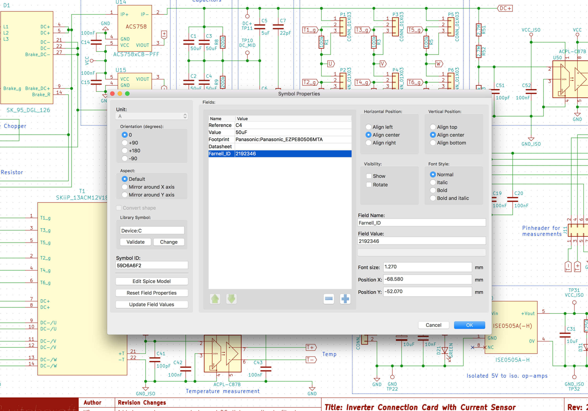
For those who are downloading the schematic from GitHub, all the non-trivial components has part number used by Element14 (also known as Newark and Farnell in different regions). This is referred to as "Farnell_ID" in the lists of fields in the component properties dialog.
The new circuit board now contains:
- A three-phased full bridge diode rectifier (Semikron SK 95 DGL 126)
- A SiC-based transistor module (Semikron SKiiP 13ACM12V18)
- DC-link capacitors with discharge resistor (Panasonic EZPE80506MTA, 50 uF)
- Snubber circuit
- Five current measurements (motor current and DC-supply current)
- DC-link voltage measurement
- Connection for braking resistor
- Connection headers for seven gate drivers (6 for main inverter + 1 brake chopper)
See the schematic for full details.
With all these features in place, this PCB can replace four different cards used previously. Earlier we designed and produced one dedicated PCB for high voltage measurement, one for three-phased current sensing, one diode rectifier board and one inverter board. The experience from those projects is now put to use in order to improve all four schematics and put them on the same PCB.
It was quite a feat to get all the electrical connections routed as there are both high power and high voltage traces mixed closely with signal traces. The DC-link voltage can be up to 1000 VDC when connected to 690 V mains (marine/offshore), but at the lab with 230 Vac, the DC-link voltage is "only" about 325 VDC.
When it comes to routing traces on an inverter PCB, it is incredible important to establish a low inductance path between the capacitors and the main transistor switches. Check out this discussion at EEV Blog Forum about the importance of these aspects. The thread starter does a pretty decent job documenting his work and troubleshooting before coming up with a well-documented solution, so be sure to read it before starting any PCB inverter design of your own.
This time I have replaced traditional traces with zones to maximize the electrical cross-section area between capacitors and switches and also between the switches and the motor output. Hopefully this will lead to high power throughput with low inductance/resistance.
Top view 3D-render. The rectangle to the left is the rectifier with a current sensor above and below. The two red office-building-like components are snubber capacitors. The black boxes on the bottom side are main DC-link capacitors while the square, white box with a copper roof at the right is the SiC transistor module with three current sensors sitting next to it.
The bottom side of the PCB contains most of the components used for the current- and voltage sensing. Also, of course, the DC-link capacitors.
Top view in 3D showing only the board with silkscreen (the white drawings and letters etc), the soldermask (the blue stuff) and the topside copper (the other stuff you can see shining trough the blue stuff, right?) Below are images shown without ray tracing for better clarity - also the bottom side is shown.


The PCB layout, showing all layers. Green are electrical connections (routes) located at the bottom side of the board while red are connections on the top side. The yellow circles all around are mounting holes with electrical connections to components with pins. One notable exception is the filled, yellow circle near the center of the board - this is a mounting hole for the transistor module.
This view highlights all the electrical connections on the top side. Here, the zones are very visible, the two largest ones are DC+ and DC- zones, while the three to the right are motor output zones to the motor terminal connector. The two small zones to the left are also DC+/-, but before the current sensor.
This view highlight the connections on the bottom side. Mostly control circuitry, but the thick ones in the upper left corner belongs to the main AC supply into the rectifier.
The circuit schematic for the whole board. Use to blue comments on the drawing to get an idea about what's what.
If you are using KiCad, this project - along with everything else - can be downloaded/cloned from GitHub. If you are not using KiCad, you should. It's free, its open source, it is used by cern and it is very powerful. Also, all the libraries for symbols, footprints and 3D-models are free and easily accessible.
Some footprints and 3D-models were not available when making this PCB (Semikron components, DC-link capacitors). These where made by us at Switchcraft and are available in a separate repository at GitHub.
Below are photographs of the four existing PCBs which hopefully can be fully replaced by the new card. I sketched up the dimmensions of the board on my notebook and placed some of the components on it to get a feel about how it would be.


I will now leave the PCB design alone for a few days and then check back into it before ordering it in case there are some bugs left. Also Eirik, the co-writer on this side, will do a side man check for me in case there are some obvious design flaws or connection errors.
It will be around $ 125 including shipment and local taxes from Seeedstudio. We were quite happy with the production quality the last time, so I see no reason to change.
Yngve out